
Results: Project Debugging of Real-Time Systems
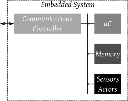
During the two year run of the project "Debugging of Real-Time Systems" a system-on-chip (SoC) with special enhancements to facilitate the process of distributed debugging was created. Based on the fact that today's solution of debugging and testing distributed system do not emphasize the distributed character of the system enough, an SoC based on an open source IP core library was developed. The system consists of the building blocks of a common embedded system: a CPU connected via a system bus to its memory and peripheral components. Moreover it is connected to a communication network via a communication controller.
 |
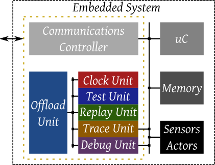
This system was then enhanced to enable non intrusive debugging. To achieve this a background debugging system was added to the architecture. It consists of an offload engine, a second CPU in charge of clock synchronization calculations and execution of debug commands, connected to certain debugging support units via a dedicated debug bus. These units are:
- a clock unit providing a globally synchronized timebase for the node
- a debug unit to gain access to the internals of the main CPU
- a trace unit to monitor transfers on the system bus
- a test unit providing access to the system bus and external units
 |
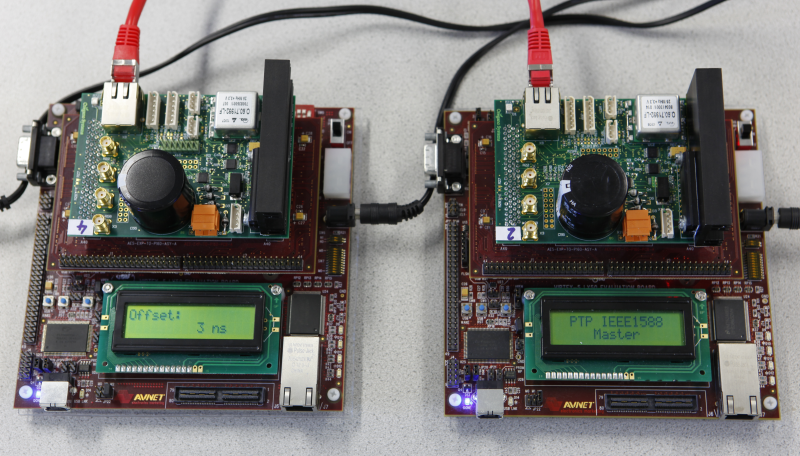
The news value of the developed concept is confirmed by the grant of a patent on its methodology. The concept is supplemented by the use of a clock synchronization algorithm which allows to perform coordinated debug actions on all the nodes in the distributed system resulting in for example a stop of the complete system at a predefined time. During the implementation of the system the world's first low hardware footprint, completely offloaded, on-chip clock synchronisation mechanism was developed and presented at the plugfest of the ISPCS 2008.
This part of the project was created in synergy with the company Oregano Systems, a company developing among other topics clock synchronization mechanisms, which provided equipment for testing and operating a synchronized distributed system.
 |
 |
| (click on the images for higher resolution) | |
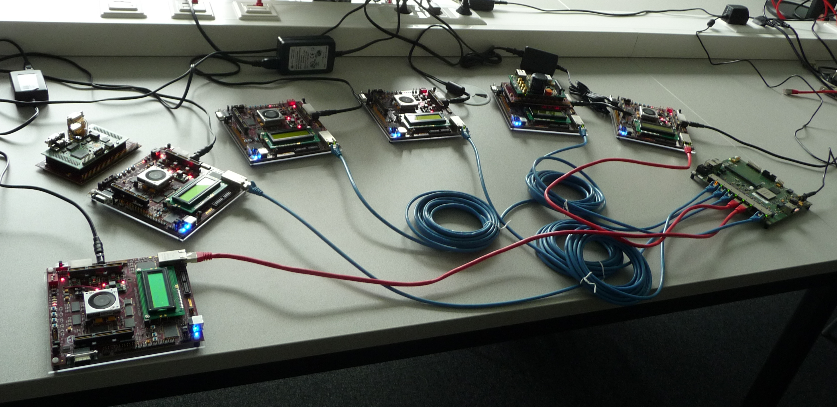
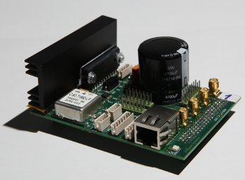
The outcome of the project was the creation of an inverted pendulum demonstrator to allow students to observe an operating distributed real-time system. To interface with the motor and sensors of the pendulum a hardware extension board had to be developed. This board was a design co-developed by members of the research project and a master student of the institute and resulted in a master thesis on the topic.
 |
The work packages in the project included
- Evaluation of the Gaisler Aeroflex Leon3 CPU
- Evaluation of the Oregano mc8051 CPU
- Specification of an architecture that allows non intrusive debugging
- Integration of the specified system
- Integration of offloaded clock synchronization methods
- Verification and test of the distributed system
- Development and bring up of hardware extension board to communicate with peripheral sensors and actuators
- Construction and bring up of inverted pendulum demonstrator
- Implementation of the operator PC software to allow centralized debugging of distributed systems
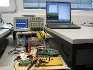
As a second part of the work in the project, automotive electronic devices of the company Continental Automotive Austria were analyzed. The task was to regenerate test signals that a window lifter board transfer through a damping resistor capacitor network resulting in signals with peak to peak voltages of a few Millivolts. The very low signal to noise ratio and the high frequency of the signal made it necessary to create an FPGA design which allows to reconstruct the signal
 |
The work packages in this part of the project included
- Evaluation of the electronic device and its output signal
- Development of a regeneration circuit allowing the FPGA to detect edges in the signal
- Implementation of FPGA design to extract information from regenerated signal and transfer data to PC
- Implementation of analysis software on PC to check incoming data
- Verification and test of the design
- Test of design in real world environment
This part of the project resulted in the delivery of intense measurement protocols and a prototypical circuit setup, which is capable of regenerating the signals transferred from the provided electronics, to Continental Automotive Austria, where the development will be used to speed up the search for software errors.