
Results
Besides the developed course materials (lecture notes, demo examples, EDA tool flows and scripts ...) which greatly ease design and verification steps in future student projects, a 8051-based microcontroller was designed and implemented as a standard-cell ASIC in a 0.35um (C35B4) CMOS process technology.
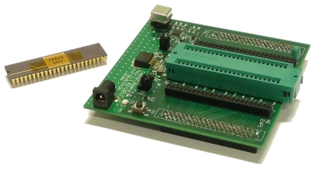
A number of 40 prototype samples have been manufactured by ams (formerly austriamicrosystems) in Unterpremstätten, Austria (see left side of figure). Moreover, a PCB was designed which contains a zero-force socket for the ASIC samples, a clock circuitry (oscillator, PLL), a power supply for the ASIC a reset generator as well as several extension/prototype headers (see right side of figure). The PCB is not only intended to be used for the 8051 ASIC but also as a test platform for future ASIC designs.
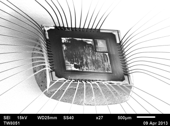
The figure on the left side shows a photo of the 8051 ASIC which was made by the use of a electron microscope. One can see the chip which is glued into the cavity of the DIL package. The IO pads are located around the core and connect the die to the IO pins via the bond wires. The memory of the microcontroller is held in the upper right corner of the chip. The total chip area is about 5 square millimeters. Many thanks go to the Department of Biochemical Engineering for providing the microscope!